-
Mfm Kevlar Mapping Annealed membrane Boundary Techcomp semifluorinated alkane TyphimuriumBiofilm block_copolymer UnivMaryland flakes Bismuth BariumTitanate LiIonBattery Indium_tin_oxide Yttria_stabilized_Zirconia C36H74 DentalProsthesis OpticalModulator NtuEee BCZT BismuthFerrite Formamidinium_lead_iodide Cobalt Electical&Electronics ElectrostaticForceMicroscopy Step NCM Current Gallium_Arsenide Sperm SKPM PetruPoni_Institute CuSubstrate
Report image
If you found this image unacceptable, please let us know. We will review your report and take action if we determine this image is really unacceptable.
Atomic steps on GaP(Gallium Phosphide) layer on Si
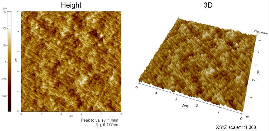
Scanning Conditions
- System: NX20
- Scan Mode: Non-contact
- Cantilever: PPP-NCHR (k=42N/m, f=300kHz)
- Scan Size: 5μm×5μm
- Scan Rate: 1Hz
- Pixel: 512×512