-
layers Steps SurfaceChange MultiferroicMaterials Cross-section Styrene SingleLayer semifluorinated_alkanes Silver bias_mode PhthalocyaninePraseodymium Hole Metal-organicComplex CHRYSALIS_INC PolymerPatterns CVD AM-KPFM NTU ThermalProperties DNA BariumTitanate HBN MechanicalProperty DNAProtein Croatia LiftHeight SrO Gallium_Arsenide China Dr.JurekSadowski temp HardDisk Mosfet MolecularSelfAssembly Protein
Report image
If you found this image unacceptable, please let us know. We will review your report and take action if we determine this image is really unacceptable.
Semiconductor device, W-plug
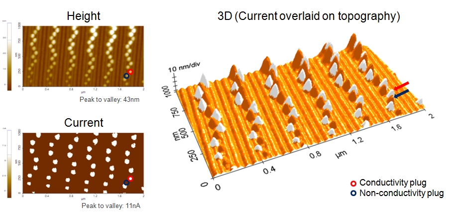
Scanning Conditions
- System: NX10
- Scan Mode: Conductive AFM
- Cantilever: ElectriMulti75-G (k=3N/m, f=75kHz)
- Scan Size: 2μm×1μm
- Scan Rate: 0.3Hz
- Pixel: 512×256
- Sample bias: +1V