-
Tin sulfide Patterns Alloy Steps Bio ScanningKelvinProbeMicroscopy RedBloodCell Al2O3 PolymerPatterns Magnets CHRYSALIS_INC ShenYang IndiumTinOxide InorganicCompound Dimethicone Titanate Hair ChemicalCompound AM-KPFM Organic Modulus domain_switching NCM\ TungstenThinFilmDeposition NanoLithography WPlug Nanostructure ElectrostaticForceMicroscopy solar_cell Praseodymium ContactModeDots fifber Yttria_stabilized_Zirconia DNA SingleCrystal
Report image
If you found this image unacceptable, please let us know. We will review your report and take action if we determine this image is really unacceptable.
Atomic steps on GaP(Gallium Phosphide) layer on Si
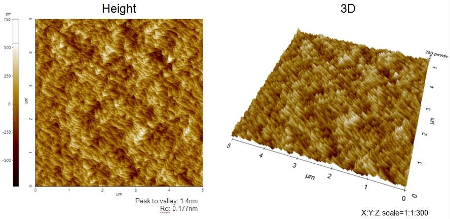
Scanning Conditions
- System: NX20
- Scan Mode: Non-contact
- Cantilever: PPP-NCHR (k=42N/m, f=300kHz)
- Scan Size: 5μm×5μm
- Scan Rate: 1Hz
- Pixel: 512×512