-
Hysteresys NCM HDD Conductance KelvinProbeForceMicroscopy TPU Au111 hetero_structure oxide_layer BFO SetpointMode Phosphide Hexylthiophene molecular_beam Worcester_Polytechnic_Institute sputter exfoliate Ceramic PVAP3HT Styrene Fe_film EFM Jason Heat ImideMonomer Stiffness GaN ShenYang margarine ThermalProperties Ceramics HfO2 PolyvinylAcetate MfmAmplitude MeltingPoint
Report image
If you found this image unacceptable, please let us know. We will review your report and take action if we determine this image is really unacceptable.
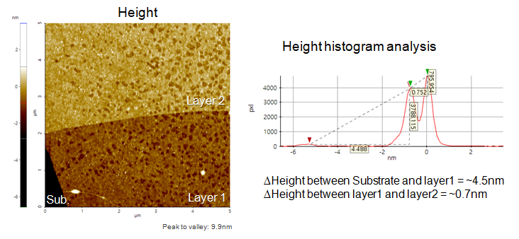
MoS2 Layers on SiO2
Scanning Conditions
- System: NX10
- Scan Mode: Non-contact
- Cantilever: AC160TS (k=26N/m, f=300kHz)
- Scan Size: 5μm×5μm
- Scan Rate: 1Hz
- Pixel Size: 256 × 256
- Scan Mode: Non-contact
- Cantilever: AC160TS (k=26N/m, f=300kHz)
- Scan Size: 5μm×5μm
- Scan Rate: 1Hz
- Pixel Size: 256 × 256