-
norganic PS_PVAC bias_mode Metal-organicComplex KevlarFiber Foil ThermalProperties Wonseok Lateral BiFeO3 HighAspect MagneticArray aluminum_nitride YszSubstrate Array Ananth TemperatureControl PFM SKPM Fujian vertical_PFM GlassTemp KAIST Cell RedBloodCell PtfeMembrane oxide_layer CeramicCapacitor DOE Growing CalciumHydroxyapatite MolybdenumDisulfide PvdfBead medical Sadowski
Report image
If you found this image unacceptable, please let us know. We will review your report and take action if we determine this image is really unacceptable.
Taegeuk Mark Lithography on PZT
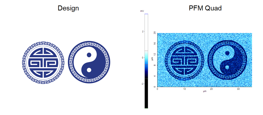
Re-arranged the domain pole direction on PZT surface using bias mode of lithography.
Scanning Conditions
- System: NX10
- Scan Mode: Lithography
- Cantilever: PPP-ContScPt (k=0.2N/m, f=25kHz)
- Scan Size: 35μm×20μm
- Scan Rate: 0.5Hz
- Pixel Size: 1024 × 1024
- Tip Bias: 10V for patterned area
- Scan Mode: Lithography
- Cantilever: PPP-ContScPt (k=0.2N/m, f=25kHz)
- Scan Size: 35μm×20μm
- Scan Rate: 0.5Hz
- Pixel Size: 1024 × 1024
- Tip Bias: 10V for patterned area