-
Ram Singapore GaAs heterojunctions CaMnO3 GalliumPhosphide SiWafer atomic_steps MagneticPhase ShenYang ImideMonomer cannabis Global_Comm Photovoltaics ConductingPolymer Gold Nanofiber Mapping SKPM Pinpoint PFM exfoliate HighAspect PS_PVAC Blend PFM thermoplastic_elastomers Vacuum Filter Carbon Change IMT_Bucharest Switching ForceVolumeImage SThM Fluoride
Report image
If you found this image unacceptable, please let us know. We will review your report and take action if we determine this image is really unacceptable.
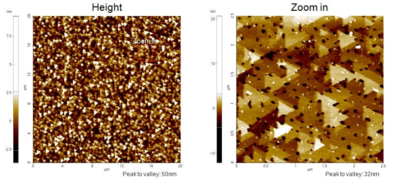
LiNbO3 wafer
Scanning Conditions
- System: NX10
- Scan Mode: Non-contact
- Cantilever: AC55TS (k=85N/m, f=1600kHz)
- Scan Size:20μm×20μm, 2.5μm×2.5μm
- Scan Rate: 5Hz, 10Hz
- Pixel: 512×512, 256×256
- Scan Mode: Non-contact
- Cantilever: AC55TS (k=85N/m, f=1600kHz)
- Scan Size:20μm×20μm, 2.5μm×2.5μm
- Scan Rate: 5Hz, 10Hz
- Pixel: 512×512, 256×256