-
Conductive AFM NusEce CrystalGrowing Implant CntFilm Temperature LateralPFM HexacontaneFilm Wafer Pinpoint PFM LiIonBattery Sadowski Oxide CVD Co/Cr/Pt InsulatorFilm Graphene ItoGlass Bismuth Metal-organicComplex OxideLayer Celebration Etch WPlug HighAspect NtuEee TungstenDeposition sputter CuSubstrate Conduct Wang polymeric_arrays DNAProtein Ceramics MagneticPhase
Report image
If you found this image unacceptable, please let us know. We will review your report and take action if we determine this image is really unacceptable.
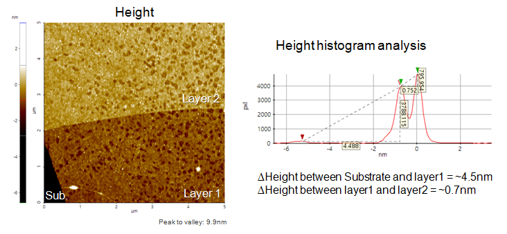
MoS2 Layers on SiO2
Scanning Conditions
- System: NX10
- Scan Mode: Non-contact
- Cantilever: AC160TS (k=26N/m, f=300kHz)
- Scan Size: 5μm×5μm
- Scan Rate: 1Hz
- Pixel Size: 256 × 256
- Scan Mode: Non-contact
- Cantilever: AC160TS (k=26N/m, f=300kHz)
- Scan Size: 5μm×5μm
- Scan Rate: 1Hz
- Pixel Size: 256 × 256