-
FM-KPFM HexagonalBN Collagen block_copolymer Cobalt PolymerPatterns PS_PVAC TemperatureControl Granada CrAu Switching Silicon ChemicalCompound PhthalocyaninePraseodymium hydrocarbon Sphere HydroGel AM-KPFM CompactDisk TiO2 ForceVolumeMapping Permalloy NUSNNI CeramicCapacitor 2dMaterials SmalScan Array cannabidiol Chloroform mfm_amplitude PhaseChange IMT_Bucharest LiBattery Self-assembledMonolayer non_contact
Report image
If you found this image unacceptable, please let us know. We will review your report and take action if we determine this image is really unacceptable.
ITO Film Sputter Deposited onto Silicon
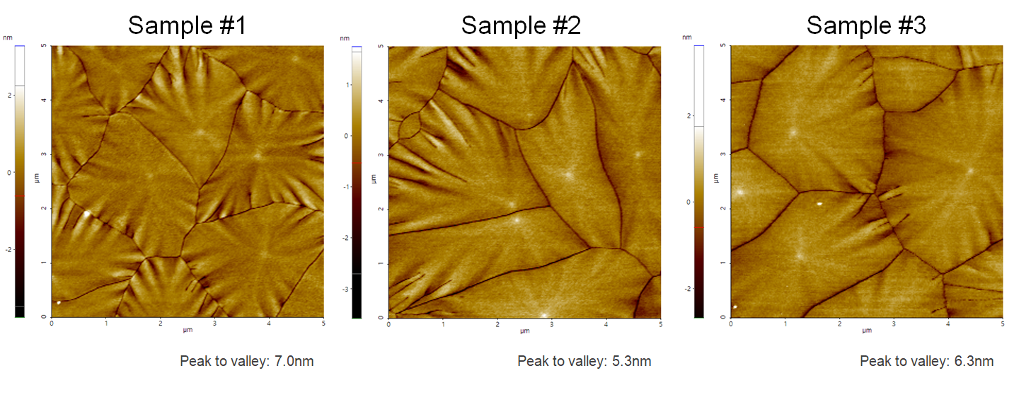
ITO-film, which was sputter deposited onto silicon. The grain size of those samples was influenced by changing the process settings in the Cluterline RAD sputter deposition system, one of the deposition tool platforms manufactured by Evatec.
Scanning Conditions
- System: NX10
- Scan Mode: Non-contact
- Cantilever: PPP-EFM (k=2.8N/m, f=75kHz)
- Scan Size: 5μm×5μm
- Scan Rate: 0.1Hz
- Pixel Size: 256 × 256
- Scan Mode: Non-contact
- Cantilever: PPP-EFM (k=2.8N/m, f=75kHz)
- Scan Size: 5μm×5μm
- Scan Rate: 0.1Hz
- Pixel Size: 256 × 256