-
DIWafer China Temasek_Lab neodymium_magnets thermal_property MoirePattern Step CeramicCapacitor Memory Roughness EvatecAG Copper CompactDisk Strontium Hysteresys SelfAssembly Lift Heating dichalcogenide Vanadate dielectric trench Cobalt-dopedIronOxide phase_change biocompatible tip_bias_mode SICM FM-KPFM WWafer SThM DentalProsthesis CVD cannabinoid Granada Imprint LiquidImaging
Report image
If you found this image unacceptable, please let us know. We will review your report and take action if we determine this image is really unacceptable.
Taegeuk Mark Lithography on PZT
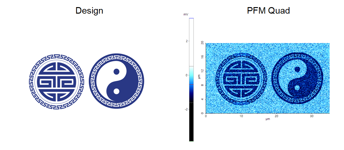
Re-arranged the domain pole direction on PZT surface using bias mode of lithography.
Scanning Conditions
- System: NX10
- Scan Mode: Lithography
- Cantilever: PPP-ContScPt (k=0.2N/m, f=25kHz)
- Scan Size: 35μm×20μm
- Scan Rate: 0.5Hz
- Pixel Size: 1024 × 1024
- Tip Bias: 10V for patterned area
- Scan Mode: Lithography
- Cantilever: PPP-ContScPt (k=0.2N/m, f=25kHz)
- Scan Size: 35μm×20μm
- Scan Rate: 0.5Hz
- Pixel Size: 1024 × 1024
- Tip Bias: 10V for patterned area