-
Ferroelectric CalciumHydroxyapatite NCM\ DeflectionOptics Pore tip_bias_mode blended polymers InsulatorFilm C36H74 AdhesionEnergy Fujian MeltingPoint ThermalConductivity HighAspect ForceVolumeImage BiVO4 Molybdenum_disulfide TriGlycineSulphate BCZT HBN Corrosion Regensburg Bacteria GaN Memory Calcium Wildtype Thermoplastic_polyurethane Mechinical GaAs non_contact CuSubstrate Imprint SmallScan TCS
Report image
If you found this image unacceptable, please let us know. We will review your report and take action if we determine this image is really unacceptable.
Monolayer Graphene on PDMS Surface
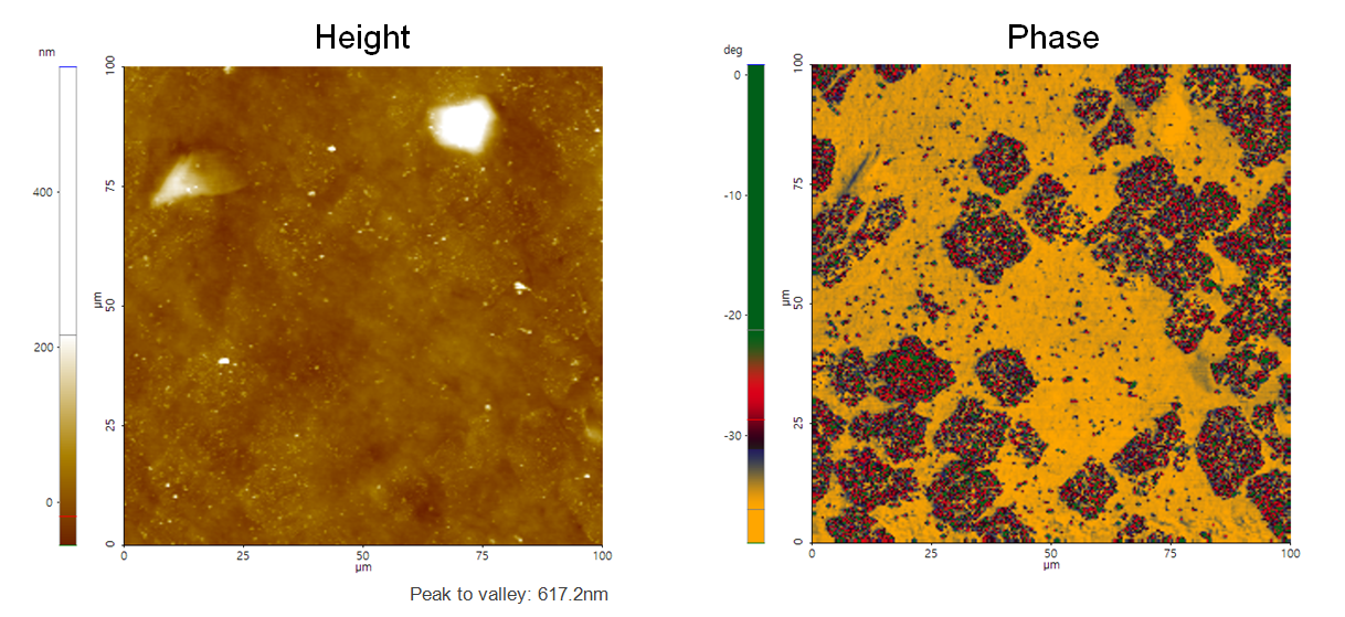
Monolayer Graphene grown on Cu foil using CVD process is transferred on to PDMS substrate.
Scanning Conditions
- System: NX20
- Scan Mode: Tapping
- Cantilever: Access-NC (k=113N/m, f=330kHz)
- Scan Size: 100μm×100μm
- Scan Rate: 0.6Hz
- Pixel Size: 256 × 256
- Scan Mode: Tapping
- Cantilever: Access-NC (k=113N/m, f=330kHz)
- Scan Size: 100μm×100μm
- Scan Rate: 0.6Hz
- Pixel Size: 256 × 256