-
ContactModeDot ScanningIon-ConductanceMicroscopy Inorganic MeltingPoint CalciumHydroxide PrCurve TappingMode TemperatureControl fluoroalkane Nanotechnology Alloy Hafnia LateralPFM LaAlO3 PvdfBead LightEmiting Ni81Fe19 BoronNitride CaMnO3 CVD TempControl temperature_control Tape ShenYang MultiLayerCeramicCapacitor LMF Platinum ImideMonomer Lateral_Force_Microscopy FrictionalForce Filter FFM mechanical_property Blend F14H20
Report image
If you found this image unacceptable, please let us know. We will review your report and take action if we determine this image is really unacceptable.
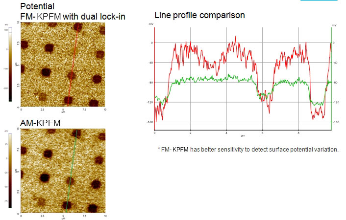
Polymer patterns on Si (2/2)

Scanning Conditions
- System: NX10
- Scan Mode: KPFM
- Cantilever: NSC36Cr-Au (k=1N/m, f=90kHz)
- Scan Size: 10μm×10μm
- Scan Rate: 0.2Hz
- Pixel: 512×256
