From automatization in research to quality control for industrial applications - April, 22, 2020
From automatization in research to quality control for industrial applications
(NX20 Large Sample AFM)
Wednesday, 22 April 2020
- 9:30 am – 10:30 am
(GMT)
London, Dublin - 10:30 am – 11:30 am
(CEST)
Berlin, Paris, Rome - 17:30pm – 18:30 pm
[UTC+9]
Seoul, Tokyo -
Learn how automation features in AFM can easily be implemented into your workflow to boost the productivity in your lab.
Our XEA software is designed to acquire accurate and repeatable nanoscale images of target devices according to user-defined procedures in custom recipe files. Utilizing a powerful combination of high-resolution digital CCD camera and pattern recognition software, a fully automated pattern recognition and alignment is made possible for user applications. Through the user-defined recipe, created by combining this optical pattern recognition and the precision of the AFM, accurate and repeatable nanoscale metrology with quantifiable data via automated data acquisition and analysis can be performed.
The corresponding increase in productivity makes this combined software and hardware solution attractive for multiple fields in nano-scaled surface optimization. Fields such as wafer manufacturing (surface roughness) and wafer design research (critical dimension measurement) are two examples of industry and research areas that systematically incorporate a tool capable of fully automated AFM to tune or control their processes and thereby increase the efficiency. Given this ability to automate data acquisition and analysis, this process has a viable application in similar fields.
Presented By :
Dr. Victor Bergmann, Application Director at Park Systems Europe, Mannheim, Germany
bergmann@parksystems.com
Victor Bergmann is the Technical Director at Park Systems Europe, where he is leading the team of application and service engineers. Before he joined Park Systems, he spent his PhD at the Max-Planck-Institute for Polymer Research in Mainz in the group of Hans-Jürgen Butt. His main research topic was studying different kinds of solar cells by means of Kelvin Probe Force Microscopy. Within the framework of the International Research Training Group 1404 he also spent half a year at Seoul National University using the AFM to characterize self-organizing nanostructures. As he just recently defended his thesis, he is now waiting for the corona shutdown to end to officially receive his doctoral degree.
Full-automation AFM in-line capabilities with the NX-Wafer - May, 6, 2020
Wednesday, 6 May 2020
- 15 pm – 16 pm
(GMT)
London, Dublin - 16 pm – 17 pm pm
(CEST)
Berlin, Paris, Rome - 10am – 11am
[EDT]
Boston, New York -

In this LIVE DEMO on the NX-Wafer Automated AFM we will introduce you to the inline metrology capabilities which are needed for full-automatic quality control.
As a follow up to the previous live demo on the NX20 large sample AFM, we will introduce you to the soft- and hardware additions in the world of automation to run the tool 24/7.
Features such as automatic wafer-handling and automatic tip exchange are necessary to control the tool completely remote. Automatic data acquisition and analysis of roughness, trench width, depth, and angle measurements are some of the most common applications, but only a fraction of the various analysis possibilities. With the #1 choice of AFM’s in the market you can be sure to find the perfect metrology solution for quantitative nano- to sub-nanoscale process inspection.
This LIVE DEMO will give you a solid overview of the high productivity and powerful features for inline wafer-fab metrology provided by NX-Wafer.
Presented By :
Dr. Victor Bergmann, Application Director at Park Systems Europe, Mannheim, Germany
bergmann@parksystems.com
Victor Bergmann is the Technical Director at Park Systems Europe, where he is leading the team of application and service engineers. Before he joined Park Systems, he spent his PhD at the Max-Planck-Institute for Polymer Research in Mainz in the group of Hans-Jürgen Butt. His main research topic was studying different kinds of solar cells by means of Kelvin Probe Force Microscopy. Within the framework of the International Research Training Group 1404 he also spent half a year at Seoul National University using the AFM to characterize self-organizing nanostructures. As he just recently defended his thesis, he is now waiting for the corona shutdown to end to officially receive his doctoral degree.
Recent Innovations in Scanning Tunneling Microscopy (STM) and Park SmartScan - Monday, April 20, 2020
Recent Innovations in Scanning Tunneling Microscopy (STM) and Park SmartScanTM
(Chinese/中文)
Monday, April 20, 2020 9:00-10:00(CST) Beijing
*Note: This webinar will be presented in Mandarin /中文
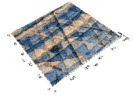
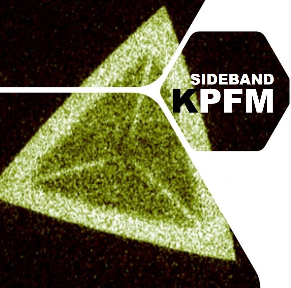
STM of Gold
Scanning Tunneling Microscopy image of Au (111) showing flat typical (111) triangular terraces.
The applications team at Park Systems is proud to present an introduction to Scanning Tunneling Microscopy (STM), a characterization technique that can achieve atomic resolution both vertically and horizontally. STM utilizes a sharp conducting tip and applies a bias voltage between the tip and the sample. When the tip is brought close to the sample, tunneling current occurs and changes exponentially as distance increases, thus providing a remarkably high resolution.
This webinar will explain the basics of STM and review ambient and liquid STM experiments using Park NX series AFM systems. More recent advances in our powerful data analysis software, SmartScan, will be introduced, including PinPoint mechanical mode Nanolithography functions.
Speaker:
Jiali Zhang, Ph.D., Applications Engineer, Park Systems
Jiali Zhang, Ph.D., is an engineer for Park Systems, where she focuses on the installation and support of AFM systems for Park’s research user base. She is also responsible for researching and writing technical papers and application notes for publication and presentation at scientific conferences. She received her Ph.D. in Analytical Chemistry from the University of California, Davis, and holds a B.S. in Applied Chemistry from Donghua University in Shanghai, China. Her expertise spans numerous microscopy techniques, and areas of study have also included biological systems and 3D printing technologies.
Advanced Piezoresponse Force Microscopy – optimizing PFM for your applications from off resonance to frequency tracking - April 29, 2020
Advanced Piezoresponse Force Microscopy –
optimizing PFM for your applications from off resonance to frequency tracking
Wednesday, 29 April 2020
- 10:00 am – 11:30 am
(GMT)
London, Dublin - 11:00 am – 12:30 pm
(CEST)
Berlin, Paris, Rome - 18:00pm – 19:30 pm
[UTC+9]
Seoul, Tokyo -
The application the ferroelectric materials in communication and information technology or data storage continuously increases. The optimization ferroelectric devices and investigation of novel applications, such as energy harvesting, are of great interest for the scientific community and require characterization techniques that can access nanoscopic domain patterns. Here, piezoresponse force microscopy (PFM), a contact mode Atomic Force Microscopy method, provides real-space domain information with a nanometer resolution.
In this webinar, we provide an overview and introduction of three available PFM modes: Off-resonance single frequency PFM, resonance-enhanced single frequency PFM and dual frequency resonance tracking (DFRT) PFM. Each of the modes comes with advantages and disadvantages depending on the piezoelectric and topographic properties of the investigated samples. To help you exploit the full potential of PFM, we will to provide you with the information which mode is most suitable for your samples.
Presented By :
Ilka Hermes - Principle Scientist Park Systems Europe, Mannheim, Germany
ihermes@parksystems.com
Ilka is the principle scientist at Park Systems Europe, where she maintains and supports scientific collaborations to establish new research projects.
Prior, she worked at the Max Planck Institute for Polymer Research (Main Germany) in the group of Stefan Weber to investigate perovskite solar cells with electrical Atomic Force Microscopy (AFM) modes, and at the Johannes Gutenberg University Mainz in the group of Angelika Kühnle to characterize liquid-solid interfaces with high resolution AFM. Ilka’s primary fields of expertise include Piezoresponse Force Microscopy (PFM), Kelvin Probe Force Microscopy (KFM), and conductive AFM on semiconducting and/or ferroelectric devices.
Exploring the Potential of the Sideband KPFM Mode - April 9, 2020
Advances in Materials Nanocharacterization and Material Analysis
Exploring the Potential of the Sideband KPFM Mode
Andrea Cerreta1, Ilka Hermes1, Victor Bergmann1, Charles Kim2
Thursday, 9 April 2020
- 10:00 am – 11:30 am
(GMT)
London, Dublin - 11:00 am – 12:30 pm
(CEST)
Berlin, Paris, Rome - 18:00pm – 19:30 pm
[UTC+9]
Seoul, Tokyo -
Abstract
Kelvin Probe Force Microscopy (KPFM) is a scanning probe method that utilizes electrostatic forces between a nanoscopic, conductive tip and a sample for material characterization by mapping the distribution of the surface potential [1,2].
In the standard lift mode KPFM [3], the sample is first scanned in dynamic mode at close distance in order to retrieve its topography. During the second pass, the tip is retracted at a given lift distance and traces back the topography while electrically excited at the lever eigenmode frequency. Since the conductive tip is sensitive to the local gradient of the electrical field, one can minimize the amplitude or phase shift of the probe caused by such a gradient by applying a counteracting voltage on the tip, which would exactly compensate the sample potential at each pixel. This allows to detect and image the potential variation along each line of the scanned frame.
However, this dual-pass mode has several technical drawbacks. First, due to the lift height the electrical signal measured by the tip is necessarily an averaged contribution of a larger area of the sample during second pass, which implies a loss in lateral resolution. Second, since the tip needs to scan each line twice, a longer image acquisition time must be taken into account. On the other hand, a simultaneous mechanical and electrical excitation of the lever at its resonant frequency would cause a severe crosstalk between topographic and electrical signals.
The new sideband KPFM mode allows for simultaneous imaging of the topography and surface potential with a high spatial potential resolution and improved sensitivity with respect to lift mode and other KPFM (e.g. off-resonance) methods. Here, the topography is detected at the resonance of the cantilever, while the electrical drive of the KPFM is applied at much lower frequencies between 1 and 4 kHz. Due to frequency mixing, satellite peaks or sidebands appear in 1 and 4 kHz from the resonance. The parallel detection of both excitations is feasible due to the presence of multiple lock-ins in the Park NX default electronics. Since the KPFM signal is detected on the sidebands and the topography is detected on the resonance, both signals can be measured simultaneously.
This webinar will provide a theoretical introduction to KPFM and show live examples of sideband KPFM experiments using the Park NX20 Large Sample AFM.
[1] U. Zerweck et al., Phys. Rev. B 71 (2005) 125424.
[2] A. Axt et al., Beilstein J. Nanotechnol. 9 (2018) 1809-1819.
[3] H. O. Jacobs et al., Ultramicroscopy 69 (1997) 39-49.
Presented By :
Dr. Andrea Cerreta - Application Scientist Park Systems Europe, Mannheim, Germany
acerreta@parksystems.com
Dr. Andrea Cerreta is an Application Scientists at Park Systems Europe, where he focuses on application development and support for the academic sector. He received his Ph.D. in Physics from the Ecole Polytechnique Fédérale de Lausanne (EPFL), Switzerland. He did his further doctoral work at the Solid State Physics Group of Université de Fribourg, Switzerland, which focused on studying electrical and magnetic properties of organic spin valves and spin polarized currents in superconducting materials, grown by means of Pulsed Laser Deposition, and characterizing the DC and AC transport properties of magnetic and superconducting samples. His expertise also spans the Frequency Modulation Atomic Force Microscopy in UHV for the study of biomolecules.