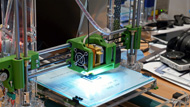
3D Printing: Testing for Mechanical Properties - June 19, 2020
Friday, June 19, 2020
- 9:00 am – 10:00 am
(PDT)
San Francisco, LA - 12:00 pm – 13:00 pm
(EDT)
Boston, New York - 5:00 pm – 6:00 pm
(GMT)
London - 6:00 pm – 7:00 pm
(CET)
Paris, Rome
Testing for 3D Printing
As additive manufacturing becomes more widespread, the standardization of materials testing, including thermomechanical properties is required.
The Park Systems 2020 Material Science Research and AFM Webinar Series continues.
As the engineering and R&D of new materials progresses, industry and academia are working together to standardize the testing of materials, an important step for improving function and applications. Thermomechanical properties testing is a requirement as additive manufacturing moves beyond prototyping and into actual parts production.
This is the third webinar in our 2020 Material Science Research and AFM Webinar Series, designed to help researchers understand leading edge developments in Materials Science Research and Applications using Atomic Force Microscopy. To view videos of previous Park Systems’ webinars, click the titles on our webinar page.

Presented By :
Prof. Rigoberto Advincula, Macromolecular Science and Engineering, Case Western Reserve University
Dr. Advincula is a Professor with the Department of Macromolecular Science and Engineering at Case Western Reserve University and Editor-in-Chief of MRS Communications, Materials Research Society. He was formerly Chair of the Polymer Chemistry Division, American Chemical Society (ACS). He is recognized industry-wide as an expert regarding polymer and materials and is also a member of NACE, SPE, ACS. Dr. Advincula is the recipient of numerous awards including Fellow of the American Chemical Society, Herman Mark Scholar Award of the Polymer Division, and Humboldt Fellow. More recently, he was elected Member of The National Academy of Science and Technology (Philippines). He did Post-doctoral work at the Max Planck Institute for Polymer Research and Stanford University and has published over 500 papers, including 250 peer-reviewed publications, 11 patents (and pending) – H-index of 65 with over 13,000 citations, and has co-edited the book on Functional Polymer Films, Polymer Brushes, and New Trends in Polymer Science.
Photovoltaic effect in ferroelectric materials (by using Piezoresponse Force Microscopy PFM) - June 17, 2020
Photovoltaic effect in ferroelectric materials
(by using Piezoresponse Force Microscopy PFM)
Wednesday, 17 June 2020
- 10:00 am – 11:30 am
(GMT)
London, Dublin - 11:00 am – 12:30 pm
(CEST)
Berlin, Paris, Rome - 17:00 pm - 18.30 pm
[GMT+8]
Beijing, Singapore - 18:00 pm – 19:30 pm
[UTC+9]
Seoul, Tokyo
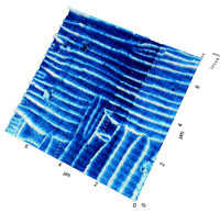
Photo-current signal acquired with Conductive-AFM from domain walls in BiFeO3
Observation of photovoltaic effect in ferroelectric thin films has been of great relevance for the field of multiferroics and photovoltaics. While this adds yet another functionality to multiferroics, generation of photocurrent in the absence any junction provides an exciting platform for studying a new charge separation mechanism. In this regard, scanning probe microscope can be considered as one of the most powerful techniques for investigating material properties on a nanoscale. The properties that can be measured are determined by the type of the probe. In the case of an electrically conductive probe, ac and dc signals can be used to analyze the photo-conductive, piezoelectric and ferroelectric character of the material.
In this talk, thin films of epitaxially grown BiFeO3 and Pb(Zr,Ti)O3 will be used to demonstrate the photoelectrical response from ferroelectric materials. Piezoresponse force microscope was utilized to confirm the ferroelectric character of the samples and analyze the domain arrangements. Macro-scale measurements were conducted to extract the photoelectrical response. A clear bulk-driven photovoltaic effect was visible in BiFeO3 films which was found to be in a rather intricate correlation with in-plane polarization. In the case of PZT films, apart from a photovoltaic effect, light induced a surprising enhancement in the conductivity of the samples which was found to decay over time, i.e. persistent photoconductivity. The results therefore showcase manifestation of two characteristics, photovoltaic effect and persistent photoconductivity, that are conventionally associated with semiconductors, in ferroelectric materials.

Presenter:
Dr. Akash Bhatnagar,
The Centre for Innovation Competence SiLi-nano®
Martin Luther University of Halle-Wittenberg, Germany
akash.bhatnagar@physik.uni-halle.de
Akash is a Group Leader at Zentrum für Innovationskompetenz SiLi-nano in Halle. The primary focus of his group is synthesis and characterization of ferroelectric/multiferroic materials for functional applications. His expertise includes thin film growth, surface probe microscopies and transport measurements. Prior to this position, Akash received his Doctorate at Max Planck Institute of Microstructure Physics while working in the group of Prof Dietrich Hesse, and subsequently worked as a Research Fellow at University of Warwick, UK in the group of Prof. Marin Alexe.
Investigation of thermoelectric material using atomic force microscopy (Chinese/中文) - May 21, 2020
May 21, 2020 10:00-11:00 (CST) Beijing
*Note: This webinar will be presented in Mandarin /中文
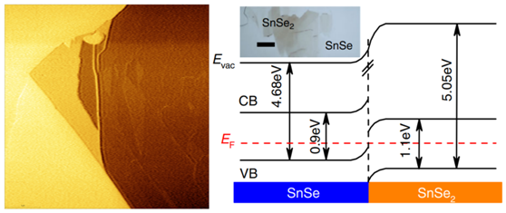
L) KPFM image of SnSe crystal surface. The color in the figure represents the measured surface potential value.
R) band alignment for SnSe and SnSe2 natural heterojunction.
Atomic force microscopy is an important tool in the research of surface topography and property, not only utilized in thin film, but also single crystal surface. Thermoelectric materials can generate electricity from waste heat, so it is environmental friendly. SnSe is a promising thermoelectric material with record-breaking figure of merit 2.6 at 923K, thus being widely used in prospect. However, the self-hole-doping mechanism in SnSe is still absent. Here we use AFM to study two kinds of defects in SnSe: SnSe2 micro domain and point dislocation. Then we provide an explanation for its self-hole-doping mechanism and electronic structure. This webinar consists of two parts: (1)Theory and operation of Kelvin probe force microscopy (2) Investigation of thermoelectric material SnSe using AFM.
Speaker:
Dr. Qifeng Hu
Qifeng Hu is currently a Ph.D. candidate in Prof. Yi Zheng in Zhejiang University. His research interests focus on 2D material multi-iron parts and electron transport. He has participated 3 SCI papers, and won the first prize of doctoral admission scholarship of 2011 collaborative innovation center.
SmartScan SICM Imaging - May 29, 2020
Friday, May 29, 2020
- 3:00 pm
(EDT)
Boston, New York - 12:00 pm
(PDT)
San Francisco, LA - 8:00 pm
(GMT)
London - 9:00 pm
(CET)
Paris, Rome
SICM ARS Mode
Topography and (b) contrast enhanced topography images of collagen sample imaged in PBS solution with SICM ARS mode. Individual fibril can be clearly identified and the thinnest one observed is about 90nm in width, as pointed by the black arrow. Scan size 10µm×10µm. Image size 256 px× 256 px.
Atomic Force Microscopy (AFM) uses a feedback loop to obtain nanoscale resolution images. This feedback is reliant on keeping a parameter constant. In contact-based imaging this is a constant force and in True Non-Contact™ imaging, an amplitude of a resonance at a given frequency. In Scanning Ion Conductance Microscopy (SICM), the cantilever is replaced with a pipette, filled with ionic fluid and the flow of ions kept constant, which generates a measurable current, allowing another imaging technique using similar principles to AFM. This session will demonstrate this technique and focus on Approach Retract Scanning (ARS) to image with a pipette using Park Systems AFM.

Presented By :
Presented By : Ben Schoenek, Park Systems Sr. Technical Service Engineer
Ben Schoenek is a Senior Technical Service Engineer for Park Systems, where he focuses on service and support of AFM systems for Park’s research user base. He received his Master’s in Physics from Auburn University, and holds a B.A. in Physics from Kenyon College.
SmartScan Lithography - May 22, 2020
Friday, May 22, 2020
- 3:00 pm
(EDT)
Boston, New York - 12:00 pm
(PDT)
San Francisco, LA - 8:00 pm
(GMT)
London - 9:00 pm
(CET)
Paris, Rome
Creating nanometer sized structures with ease
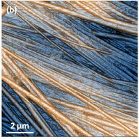
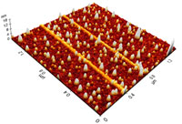
3D image of oxide patterns formed through Park AFM Nanolithography.
Park AFM’s nanolithography is an advanced AFM technique used to pattern nanoscale shapes onto sample surfaces. In the bias-assisted or anodic oxidation method, a bias voltage is applied to the tip to generate an oxide pattern on a metallic or semiconductor substrate. In this session, we will demonstrate how to create nanometer sized structures and discuss the main parameters to consider during the process using SmartScan™ Nanolithography on the Park NX10 AFM system.

Presented By :
Presented by Armando Melgarejo, Park Systems Technical Support Engineer
Armando Melgarejo is an engineer for Park Systems, where he focuses on the installation and support of AFM systems for Park’s research user base. He holds a B.S. in Biotechnology Engineering from Autonomous University of Queretaro, Mexico. During his studies, he also spent a semester doing research in nanotechnology and molecular biology at Czech Technical University in Prague, Czech Republic. Other areas of expertise include diverse characterization techniques (AFM, SEM, RAMAN and IR), genetics and molecular and cell biology.