4D Printing and Stimuli Response - May 22, 2020
Friday, May 22, 2020
- 9:00 am – 10:00 am
(PDT)
San Francisco, LA - 12:00 pm – 13:00 pm
(EDT)
Boston, New York - 5:00 pm – 6:00 pm
(GMT)
London - 6:00 pm – 7:00 pm
(CET)
Paris, Rome
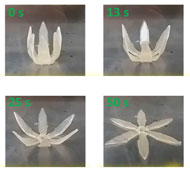
4D Printing
Four dimensional printing is the process by which a 3D printed object transforms itself into a new structure due to the influence of environmental stimuli.
The Park Systems 2020 Material Science Research and AFM Webinar Series continues.
Stimuli responsive materials offer unique properties in physico-chemical field effect, resulting in properties that can both be functional and esoteric. This webinar session will give some insights into understanding the 4D transformation of materials which govern both design of shape and material properties.
This is the third webinar in our 2020 Material Science Research and AFM Webinar Series, designed to help researchers understand leading edge developments in Materials Science Research and
Applications using Atomic Force Microscopy. To view videos of previous Park Systems’ webinars, click the titles on our webinar page.

Presented By :
Prof. Rigoberto Advincula, Macromolecular Science and Engineering, Case Western Reserve University
Dr. Advincula is a Professor with the Department of Macromolecular Science and Engineering at Case Western Reserve University and Editor-in-Chief of MRS Communications, Materials Research Society. He was formerly Chair of the Polymer Chemistry Division, American Chemical Society (ACS). He is recognized industry-wide as an expert regarding polymer and materials and is also a member of NACE, SPE, ACS. Dr. Advincula is the recipient of numerous awards including Fellow of the American Chemical Society, Herman Mark Scholar Award of the Polymer Division, and Humboldt Fellow. More recently, he was elected Member of The National Academy of Science and Technology (Philippines). He did Post-doctoral work at the Max Planck Institute for Polymer Research and Stanford University and has published over 500 papers, including 250 peer-reviewed publications, 11 patents (and pending) – H-index of 65 with over 13,000 citations, and has co-edited the book on Functional Polymer Films, Polymer Brushes, and New Trends in Polymer Science.
Advanced High Vacuum Magnetic Force Microscopy (MFM): study of topological spin textures - May 20, 2020
Advanced High Vacuum Magnetic Force Microscopy (MFM): study of topological spin textures
Wednesday, 20 May 2020
- 10:00 am – 11:30 am
(GMT)
London, Dublin - 11:00 am – 12:30 pm
(CEST)
Berlin, Paris, Rome - 17:00pm - 18.30pm
[(GMT+8]
Beijing, Singapore - 18:00pm – 19:30 pm
[UTC+9]
Seoul, Tokyo
By now, spintronics is an established field of condensed matter physics and has become an active branch in the sensor and the microelectronics industry. The discovery of the Giant Magnetoresistance in 1988 by Pr. A. Fert, who was awarded the 2007 Nobel Prize in Physics together with Pr. P. Grünberg, marks the birth of spintronics. After three decades of research, the field of spintronics still presents vivid dynamics at the fundamental level and in applications.
As such, new concepts like topological spin textures have recently arisen in the community, which could bring disruptive solutions in information-communication technologies, neuromorphic electronics, etc. The development and access to user-friendly advanced characterization tools in nanomagnetism is a key requirement to study new magnetic phenomena. In this context, magnetic force microscopy (MFM) is unique characterization technique that can image even weak magnetic signals from nanometer scale spin textures very efficiently. MFM is an atomic force microscopy method, in which a magnetized tip-cantilever system probes the magnetic properties of a surface with a nanoscale resolution. This real-space, high-resolution visualization of magnetic structures offers valuable insights for research and application of spintronics.
In this talk I’ll present you, from the Engineer point of view, the contribution of MFM in various experimental configurations to the undergoing research at UMPhy on ferromagnetic and antiferromagnetic skyrmions.
The theoretical introduction on High Vacuum MFM will be done by Ilka Hermes, Principle Scientist at Park Systems Europe.
Presented By :
Dr. Karim Bouzehouane, CNRS-Thales Joint Physics Laboratory, France
karim.bouzehouane@cnrs-thales.fr
Karim is a research engineer at CNRS-Thales joint Lab (UMPhy) led by Prof. Albert Fert. He is an expert in scanning probe microscopies. His expertise includes SPM techniques such as Conductive Tip-AFM, Piezo-Force Microscopy and Magnetic Force Microscopy. Karim is currently involved in different research fields, such as multiferroïc oxide materials, 2D materials and topological spin textures.
SmartScan MFM Imaging - May 1, 2020
Friday, May 1, 2020
- 3:00 pm
(EDT)
Boston, New York - 12:00 pm
(PDT)
San Francisco, LA - 8:00 pm
(GMT)
London - 9:00 pm
(CET)
Paris, Rome
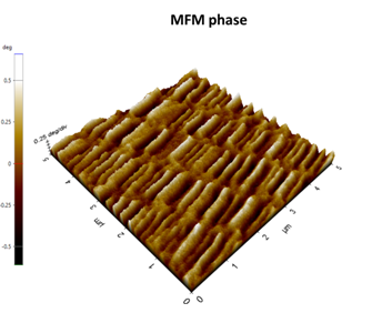
MFM phaseof hard disk
(5µm × 5µm)
Magnetic force microscopy (MFM) is a Park Systems advanced AFM mode used for studying surfaces with magnetic properties by detecting the interaction between a magnetized cantilever and the sample surface. The AFM tip is coated with a layer of magnetic coating to probe the local magnetic field thus maintaining the spatial resolution of AFM. MFM is ideal for detecting the local magnetic properties and the spatial distribution of the samples at the nanoscale. This session will demonstrate how to acquire topographic information and magnetic variations over a sample surface simultaneously by using current NX hardware and software. The basic principle, instrumentation set-up, and data analysis will be covered.

Presented By :
Jiali Zhang, Ph.D., Technical Support Engineer,
Park Systems
Jiali Zhang, Ph.D., is an engineer for Park Systems, where she focuses on the installation and support of AFM systems for Park’s research user base. She is also responsible for researching and writing technical papers and application notes for publication and presentation at scientific conferences. She received her Ph.D. in Analytical Chemistry from the University of California, Davis, and holds a B.S. in Applied Chemistry from Donghua University in Shanghai, China. Her expertise spans numerous microscopy techniques, and areas of study have also included biological systems and 3D printing technologies.
Advances in Materials Nanocharacterization: Exploring the Potential of the Sideband KPFM Mode - May 13, 2020
Advances in Materials Nanocharacterization and Material Analysis
Exploring the Potential of the Sideband KPFM Mode
Andrea Cerreta1, Ilka Hermes1, Victor Bergmann1, Charles Kim2
Wednesday, 13 May 2020
- 10:00 am – 11:30 am
(GMT)
London, Dublin - 11:00 am – 12:30 pm
(CEST)
Berlin, Paris, Rome - 17:00pm - 18.30pm
[(GMT+8]
Beijing, Singapore - 18:00pm – 19:30 pm
[UTC+9]
Seoul, Tokyo
Abstract
Kelvin Probe Force Microscopy (KPFM) is a scanning probe method that utilizes electrostatic forces between a nanoscopic, conductive tip and a sample for material characterization by mapping the distribution of the surface potential [1,2].
In the standard lift mode KPFM [3], the sample is first scanned in dynamic mode at close distance in order to retrieve its topography. During the second pass, the tip is retracted at a given lift distance and traces back the topography while electrically excited at the lever eigenmode frequency. Since the conductive tip is sensitive to the local gradient of the electrical field, one can minimize the amplitude or phase shift of the probe caused by such a gradient by applying a counteracting voltage on the tip, which would exactly compensate the sample potential at each pixel. This allows to detect and image the potential variation along each line of the scanned frame.
However, this dual-pass mode has several technical drawbacks. First, due to the lift height the electrical signal measured by the tip is necessarily an averaged contribution of a larger area of the sample during second pass, which implies a loss in lateral resolution. Second, since the tip needs to scan each line twice, a longer image acquisition time must be taken into account. On the other hand, a simultaneous mechanical and electrical excitation of the lever at its resonant frequency would cause a severe crosstalk between topographic and electrical signals.
The new sideband KPFM mode allows for simultaneous imaging of the topography and surface potential with a high spatial potential resolution and improved sensitivity with respect to lift mode and other KPFM (e.g. off-resonance) methods. Here, the topography is detected at the resonance of the cantilever, while the electrical drive of the KPFM is applied at much lower frequencies between 1 and 4 kHz. Due to frequency mixing, satellite peaks or sidebands appear in 1 and 4 kHz from the resonance. The parallel detection of both excitations is feasible due to the presence of multiple lock-ins in the Park NX default electronics. Since the KPFM signal is detected on the sidebands and the topography is detected on the resonance, both signals can be measured simultaneously.
This is a prerecorded webinar. The questions asked during the session will be answered per email. It will provide a theoretical introduction to KPFM and show examples of sideband KPFM experiments using the Park NX20 Large Sample AFM. All the questions asked during the session will be answered per email.
[1] U. Zerweck et al., Phys. Rev. B 71 (2005) 125424.
[2] A. Axt et al., Beilstein J. Nanotechnol. 9 (2018) 1809-1819.
[3] H. O. Jacobs et al., Ultramicroscopy 69 (1997) 39-49.
Presented By :
Dr. Andrea Cerreta - Application Scientist Park Systems Europe, Mannheim, Germany
acerreta@parksystems.com
Dr. Andrea Cerreta is an Application Scientists at Park Systems Europe, where he focuses on application development and support for the academic sector. He received his Ph.D. in Physics from the Ecole Polytechnique Fédérale de Lausanne (EPFL), Switzerland. He did his further doctoral work at the Solid State Physics Group of Université de Fribourg, Switzerland, which focused on studying electrical and magnetic properties of organic spin valves and spin polarized currents in superconducting materials, grown by means of Pulsed Laser Deposition, and characterizing the DC and AC transport properties of magnetic and superconducting samples. His expertise also spans the Frequency Modulation Atomic Force Microscopy in UHV for the study of biomolecules.
SmartScan Advanced KPFM Imaging - April 24, 2020
Friday, April 24, 2020
- 3:00 pm
(EDT)
Boston, New York - 12:00 pm
(PDT)
San Francisco, LA - 8:00 pm
(GMT)
London - 9:00 pm
(CET)
Paris, Rome
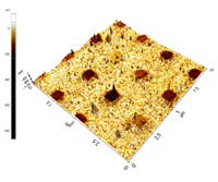
Surface Potential
3D overlay of surface potential image on topography of polymer patterned array material deposited on silicon substrate.
Park Systems Weekly Demo & Chat Sessions is a new series of online, live demonstrations of Park AFM Systems hosted by the Park Systems Technical team. Each week, an engineer from the technical team will lead a short, specific demo and then discuss it with attendees. This is the second session in the new series.
Measuring the electrostatic interaction between the atomic force microscope (AFM) tip and sample is a common technique used to characterize electrically sensitive samples. To characterize the actual potential between tip and sample, kelvin probe force microscopy (KPFM) is used. KPFM is currently standard on Park NX Series microscopes and the baseline technique is supported as the standard for KPFM. Using current NX hardware, however, it is possible to explore other advanced methods of gathering this same KPFM signal, each with their own benefits and tradeoffs. This session will demonstrate how to use advanced KPFM techniques, using current AFM hardware, and explore the advantages of working with these advanced techniques.

Presented By :
Ben Schoenek, Sr. Technical Service Engineer, Park Systems
Ben Schoenek is a Senior Technical Service Engineer for Park Systems, where he focuses on service and support of AFM systems for Park’s research user base. He received his Master’s in Physics from Auburn University, and holds a B.A. in Physics from Kenyon College.