导电原子力显微镜在电子器件纳米级电学测试中的应用 – 2020年9月24日
2020年9月24日*星期四
北京时间东八区上午9点到下午6点
*Note: This webinar will be presented in Mandarin /中文

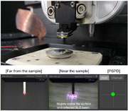
导电原子力显微镜(C-AFM)是在扫描探针显微镜(SPM)基础上扩展的一种电学测试模式,它可以同时实现在纳米级对样品(比如:介质材料、量子点、电子器件)表面形貌和局部电学性质的表征和测试。C-AFM 技术在纳米电子学、半导体材料等领域广泛应用,主要用于表征样品/器件的缺陷分布、电导率局部变化、局部电学行为等。本报告将重点围绕C-AFM在忆阻型电子器件中的电学表征,介绍不同环境(大气和真空状态)下测试结果的可靠性,以及通过使用基于C-AFM技术的不同手段来直接观测导电细丝的形成以进一步探索阻变机理。

主讲人:
惠飞,以色列理工学院,博士后研究员
惠飞博士,现以色列理工学院博士后研究员,2018年获得巴塞罗那大学和苏州大学双博士学位。在攻读博士期间,她曾先后到世界顶级名校美国麻省理工学院和英国剑桥大学进行为期12个月和6个月的访学。在科研方面,截止目前,共参与发表SCI期刊学术论文45篇。其中,一作论文13篇,包括顶级期刊Nature Electronics, Advanced Functional Materials, ACS Applied Materials & Interfaces, 2D Materials, Nanoscale等,谷歌学术论文总引用次数为1353次。参与德国Wiley出版的专著篇章一部,获国家授权发明专利两项,申请国际专利两项。担任Sensors, Electronics, Nanotechnology等期刊专刊的编委会成员、多个IEEE会议(2021 IEEE-EDTM,2021 IEEE-IPFA, 2020 IEEE-IRPS, 2020 IEEE-IIRW)的技术/宣传委员会成员、以及国际期刊审稿人。曾获得英国皇家化学会学者奖学金、2019 Park AFM博后奖学金、国家奖学金等。她的主要研究领域是基于二维材料的电子器件及其在纳米级的电学行为表征。
How to operate AFM (with live demo) - September 22, 2020
Tuesday, 22 September, 2020
- 13:30 pm
(SGT)
Singapore - 10:30 am
(PKT)
Islamabad, Pakistan - 11:00 am
(IST)
Bangalore, India - 16:30 pm
(AEDT)
Sydney, Australia
AFM Live demo
How to operate AFM
Since atomic force microscopy (AFM) has been developed, it becomes novel technique for surface investigation including topography and other material properties measurement. AFM shows high utilization in
the research field due to complementary relationships with optical microscopy, electron microscopy and other measuring equipment.
In this session, the basic principles and the application of AFM which can be used in scientific and industrial fields are examined.
In particular, we share the images measured by the actual atomic force microscope with specific examples of various applications and look at their meaning. In addition, we present how to operate AFM including cantilever
selection, sample preparation, description of imaging parameters and operation in order to obtain better understanding for AFM. As the first session, AFM cantilever selection depends on sample type is one of the most
important processes for the proper result. We review several representative AFM cantilevers and provide tips for how to choose AFM cantilever. Also, how to prepare your sample for AFM imaging, specific meaning of AFM
parameters and their outputs are discussed using actual examples and pictures.
After oral session, AFM live demo using standard sample is prepared by Park Systems skillful engineer. During the AFM live demo session, hardware and software setup with Auto and Manual mode are presented for
understanding of actual AFM measurement.
Presented By :
Jake Kim, Application Technology Center Manager, Park Systems
Dr. Kim received Ph.D. degree in Materials Science and Engineering from Nanyang Technological University, Singapore. He joined Tokyo Institute of Technology International Research Opportunities Program (TiROP) in 2014 and was engaged in nano-scale chemical composition analysis using scanning probe microscopy (SPM). From December 2017, he started to work in Park Systems as the manager of application technology center. He is specialized in the enhancement of nano-machanical measurement performance for Atomic Force Microscopy (AFM), building up a accurate and reliable environment for electrochemical measurement using Scanning Probe Microscopy (SPM; SECM,SECCM) and Scanning Ion Conductance Microscopy (SICM) applications development for biology.
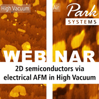
Better in Vacuum – boosting the characterization of 2D semiconductors via electrical AFM in high vacuum - September 3, 2020
Better in Vacuum – boosting the characterization of 2D semiconductors via electrical AFM in high vacuum
Thursday, 3 September 2020
- 10:00 am – 11:30 am
(GMT)
London, Dublin - 11:00 am – 12:30 pm
(CEST)
Berlin, Paris, Rome - 18:00pm – 19:30 pm
[UTC+9]
Seoul, Tokyo -
With ever-decreasing device sizes in the semiconductor industry, the demand for functional materials with low dimensionality continues to grow. Since the discovery of graphene in 2004,1 2D materials have caught
the interest of scientific and industrial research. Among 2D materials for semiconductor applications, transition metal dichalcogenides (TMDs) are particularly promising. However, TMDs often exhibit morphological
features such as grain boundaries, which affect the electronic properties locally.2 Hence, characterization of TMDs requires techniques with high spatial resolution and sensitivity for electronic properties,
including conductivity and surface potential. Atomic Force Microscopy not only offers topography imaging with local resolutions on the nanoscale, but also resolves electronic properties by scanning the surface
with an electrically conductive tip.
In this webinar, we will demonstrate on Park’s NX Hivac how high vacuum (10-5 Torr) significantly improves the sensitivity and the resolution of electrical AFM modes on TMDs.
The removal of the surface water
layer leads to an improved electrical contact between tip and sample. At the same time, the vacuum environment prevents the adverse doping effect of the TMD material, which effectively lowers the material’s
conductivity. Thereby, the local electronic characterization of TMDs can be pushed to the next level.
1.Novoselov, K. S. et al. Electric Field Effect in Atomically Thin Carbon Films. Science (80-. ). 306, 666 LP – 669 (2004).
2.Ludwig, J. et al. Effects of buried grain boundaries in multilayer MoS2. Nanotechnology 30, 285705 (2019).
Presented By :
Ilka Hermes - Principle Scientist Park Systems Europe, Mannheim, Germany
ihermes@parksystems.com
Ilka is the principle scientist at Park Systems Europe, where she maintains and supports scientific collaborations to establish new research projects.
Prior, she worked at the Max Planck Institute for Polymer Research (Main Germany) in the group of Stefan Weber to investigate perovskite solar cells with electrical Atomic Force Microscopy (AFM) modes, and at the Johannes Gutenberg University Mainz in the group of Angelika Kühnle to characterize liquid-solid interfaces with high resolution AFM. Ilka’s primary fields of expertise include Piezoresponse Force Microscopy (PFM), Kelvin Probe Force Microscopy (KFM), and conductive AFM on semiconducting and/or ferroelectric devices.
研究用AFM電気測定 EFM/KPFM - 2020年9月29日
二维材料界面结构与性质的原子力探针显微学研究(1)- 2020年8月27日
2020年8月27日*星期四
北京时间东八区上午11:00-12:00
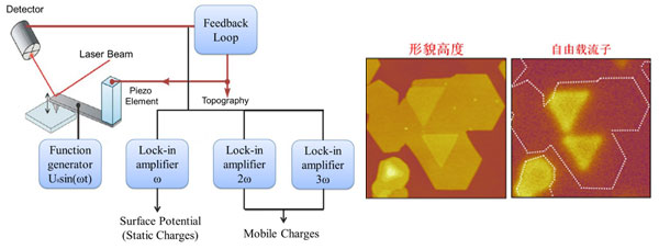
多频静电力显微术的基本原理,及其用于样品自由载流子的实空间成像探测。
近年来,由于其潜在的巨大应用价值,关于二维层状材料的基础和应用研究方兴未艾,核心工作是理解和控制其多种多样的有趣性质。之前的研究工作主要集中在二维材料的面内结构,多种多样的层间相互作用在调控其力学、电学、热学以及光学等性质方面也有重要作用。虽然已有许多实验和理论研究工作来表征和理解这些界面结构,但对于界面行为是如何影响其物理与化学行为的仍然不是特别清楚。一个重要原因是,内部界面结构的直接微观成像和性质研究在实验技术上是相对比较困难的。
在之前,报告人已经针对的AFM的基础知识、基本模式以及功能化AFM探测模式进行了介绍。本系列报告,将基于我们在原子力显微术的技术研究工作,利用多种先进原子力显微术针对二维材料的本征界面、异质界面以及材料/基底界面开展的研究工作。在每次报告中,我们首先将在较为详细地介绍主要使用的先进AFM模式的基本原理、技术实现及其相关应用。在此基础上,介绍我们利用该AFM模式所开展的关于二维材料界面结构与性质方面的研究工作。希望通过本报告有助于相关AFM使用者能够利用比较复杂的AFM功能模式开展研究工作。
主讲人:
程志海教授
中国人民大学物理学系教授,博士生导师,基金委优青,中国仪器仪表学会显微仪器分会理事,中国硅酸盐学会微纳米分会理事。2002年毕业于大连理工大学物理与光电工程学院应用物理系。2002-2007年,在中国科学院物理研究所纳米物理与器件实验室硕博连读,获凝聚态物理博士学位。2004年7月至2005年1月,在德国柏林自由大学物理系及实验物理研究所做访问学者,2007年8月-2011年7月,在美国加州大学Riverside分校化学系及纳米科学与工程中心从事博士后研究。2011年8月-2017年月,国家纳米科学中心(中科院纳米标准与检测重点实验室),任副研究员/研究员。曾获中国科学院“引进杰出技术人才计划”(技术百人计划)和首届“卓越青年科学家”,卢嘉锡青年人才奖获得者,青年创新促进会会员并获首届“学科交叉与创新奖”等。目前,主要工作集中在先进原子力探针显微分析技术及其在低维与表面物理、纳米科技等领域的应用基础研究。