-
PetruPoni FM-KPFM cannabis Nanostructure FailureAnlaysis thermal_property ContactModeDot Butterfly Mechanical&nanotechnology SolarCell Microchannel optoelectronics ScanningIon-ConductanceMicroscopy DeflectionOptics Foil Polyaniline Vanadate ForceVolume PVAP3HT Fujian sputter pulsed_laser_deposition amplitude_modulation LiNbO3 TransitionMetal Conductivity block_copolymer MagneticForceMicroscopy NUSNNI NCM doped Piezoelectric SelfAssembly Aggregated_molecules HfO2
Report image
If you found this image unacceptable, please let us know. We will review your report and take action if we determine this image is really unacceptable.
Magnetic device
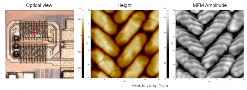
Scanning Conditions
- System : NX20
- Lift Height : 50nm
- Scan Mode: MFM
- Scan Rate : 0.3Hz
- Scan Size : 20μm×20μm
- Pixel Size : 512×256
- Cantilever : PPP-MFMR (k=2.8N/m, f=75kHz)