Lecture #9: Liquid Imaging
Magnetic Force Microscopy of nanostructures and spintronic devices
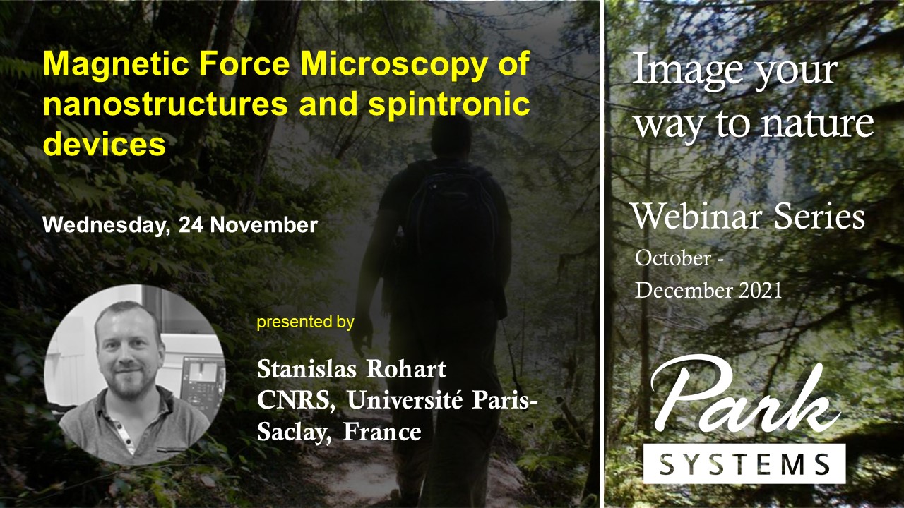
Magnetic Force Microscopy of nanostructures and spintronic devices
Wednesday, 24 November, 2021
- 10:00 am – 11:30 am
(GMT)
London, Dublin - 11:00 am – 12:30 pm
(CET)
Berlin, Paris, Rome - 18:00pm – 19:30 pm
[UTC+9]
Seoul, Tokyo

See all webinars in the “Image your way to nature” series here.
At the mesoscopic scale, magnetic materials can display a complex magnetization spatial organization that arise from the balance between exchange, anisotropy and dipolar energies. Some of these textures, like domain walls, vortices or skyrmions, behave as solitons and their motion could bring some new possibilities in spintronic devices like shift register (race track) memories or oscillators. While a numerous number of imaging techniques are available (magneto-optics, electron microscopy, x-ray based microscope and scanning probe microscopy), magnetic force microscopy (MFM) is well adapted to this field, bringing high resolution and sensitivity and easy observation of devices in-operando.
In this webinar, I will review our results on MFM imaging for textures in model nanostructures and spintronic devices. In particular, I will discuss the difficulty to deal with tip induced perturbations that are inherent to this method, and the adaptation of MFM to operate directly on electrically connected devices.
Presented By :
Stanislas Rohart, CNRS/Université Paris-Saclay, France
Stanislas is assistant researcher at CNRS/Université Paris-Saclay in France. He is interested in the physical properties of magnetic textures and their applications in spintronic applications and devices. To this purpose, he is an expert in scanning probe techniques (he has been involved into the development of magnetic ballistic electron emission microscopy and NV-center microscopy and is a common used of magnetic force microscopy). He pioneered some research on chiral magnetic textures (chiral domain walls and skyrmions), which lead to a renewed approach to this field.
Scanning Ion Conductance Microscopy (SICM)
Monday, 04 Oct, 2021
- 11:00 AM
(ARAB)
Riyadh - 1:30 PM
(IST)
New Delhi - 4:00 PM
(SST)
Singapore - 6:00 PM
(AEDT)
Sydney
Since atomic force microscopy (AFM) is developed, various applications of nanotechnology were established, and those applications have led technological advances in many science fields. Researchers can acquire detailed topography of nanostructure and accurate probe positioning and distance control in nanometer resolution. Based on those benefits from AFM’s practical imaging capability, various applications were developed and enabled many innovative material property characterizations. However, those technological advances by nanotechnology have limited in ambient environment. Very soft samples like biological samples in liquid environment, there is not much successful advances with high impact. Because of unexpected physical contact of AFM tip on sample surface, small and fragile structures can be dragged or scratched. To overcome these limitation, Scanning ion conductance microscopy (SICM) was invented. The SICM uses nano pipette with ~100 nm inner diameter as a probe and the fundamental operation of SICM relies on an ion current that flows between a pipette electrode and a bath electrode. This ion current is used as feedback signal to maintain a constant distance between the nano pipette and the sample, allowing the nano pipette to scan the surface for topography imaging with non-contact. The SICM has the advantage of being able to cover applications that are difficult to apply AFM, so it is being used in various fields such as biology, electrochemistry, material science and battery research.
Presented By :
Dr. Jake Kim, Park Systems Korea
Dr. Kim received Ph.D. degree in Materials Science and Engineering from Nanyang Technological University, Singapore. He joined Tokyo Institute of Technology International Research Opportunities Program (TiROP) in 2014 and was engaged in nano-scale chemical composition analysis using scanning probe microscopy (SPM). From December 2017, he started to work in Park Systems as the manager of application technology center. He is specialized in the enhancement of nano-machanical measurement performance for Atomic Force Microscopy (AFM), building up a accurate and reliable environment for electrochemical measurement using Scanning Probe Microscopy (SPM; SECM,SECCM) and Scanning Ion Conductance Microscopy (SICM) applications development for biology.
Lecture #8: Electrostatic modes in AFM
Intrinsic electrical characterization of two-dimensional transition metal dichalcogenides via scanning probe microscopy
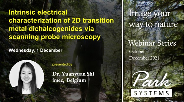
Intrinsic electrical characterization of two-dimensional transition metal dichalcogenides via scanning probe microscopy
Wednesday, 1 December, 2021
- 10:00 am – 11:30 am
(GMT)
London, Dublin - 11:00 am – 12:30 pm
(CET)
Berlin, Paris, Rome - 18:00pm – 19:30 pm
[UTC+9]
Seoul, Tokyo

See all webinars in the “Image your way to nature” series here.
In a conventional planar silicon field effect transistor (FET), the gate controllability becomes weaker when its lateral dimension becomes smaller than the transistor thickness, which results in adverse short-channel effects, including leakage current, saturation of the carrier mobility in the channel, channel hot-carrier degradation, and time-dependent dielectric breakdown. Hence, the transistor body thickness needs to be reduced to ensure efficient electrostatic control from the gate. Due to the atomic thickness and dangling bond-free surface of two-dimensional (2D) materials, theoretical studies have shown that particularly 2D transition metal dichalcogenides (TMDs), can outperform Si as the channel material, enable the atomic-level scaling, excellent electrostatic gate control, decrease off-state power consumption and further extend Moore’s Law.
Suitable techniques to characterize the intrinsic physical and electrical properties of as-deposited 2D materials, are a key link between the quality of as-deposited 2D materials and the performance of 2D materials based electronic devices. This link can help us to better understand, control and improve the performance of 2D materials-based devices. However, techniques for analyzing the intrinsic electrical properties of as-deposited 2D materials on the nanoscale without any transfer and patterning process are limited.
In this seminar, scanning probe microscopy (SPM) is used to investigate the intrinsic electrical properties of as-deposited 2D TMDs. Conductive atomic force microscope (CAFM) is performed directly on the surface of as-grown 2D materials without any patterning. CAFM allows correlating the electrical conductivity of as-grown 2D materials to their topography, thereby linking the electrical properties of 2D materials to their physical properties such as layer thickness and chemical bonds, etc. With all of this, CAFM gives us comprehensive information of as-deposited 2D materials and helps us to evaluate the impact of these intrinsic properties on 2D materials based nanoelectronics.

Presented By :
Dr. Yuanyuan Shi, imec Belgium
Dr. Yuanyuan Shi is a researcher (Marie Curie fellow) at IMEC, Belgium. She received her Ph.D. degree (with Excellent “Cum Laude” Honor and Extraordinary PhD prize) in Nanoscience from University of Barcelona in 2018. Her research interests focus on novel materials and new concepts/architectures based nanoelectronics, which target to bring new opportunities for the Post-Moore Era. Dr. Shi has published more than 60 research articles (including Nature Electronics, IEDM, ACS Nano, etc.), two book chapters and four international patents. She serves as an active committee member for IEEE EDS Nanotechnology committee and several IEEE flagship conferences, including IPFA, IRPS and EDTM. Dr. Shi also serves as a guest editor for Frontiers in Neuroscience and an active reviewer for Nature, Nature Electronics, Nature Materials, IEEE Electron Device Letters, and others. Dr. Shi is a recipient of 2020 Forbes 30 under 30 (Forbes), Marie Skłodowska-Curie Individual Fellowship (European Commission), 2020 Park AFM award (Park Systems), 2018 IEEE EDS PhD student fellowship (three winners globally each year), 2018 ADF-The Rising Stars Women in Engineering, etc.