Investigation of nanomechanical properties using AFM

Tuesday, 6 July , 2021
- 10:30 AM
(ARAB)
Riyadh - 1:00 PM
(IST)
New Delhi - 3:30 PM
(SST)
Singapore - 5:30 PM
(AEDT)
Sydney
2021 SE Asia Webinar Series Schedule:
| Date | Topic |
|---|---|
| May 25 | Principles of AFM imaging modes |
| Jun 15 | Imaging modes of AFM from the application point of view |
| Jul 6 | Investigation of nanomechanical properties using AFM |
| Aug 10 | Crosstalk-free ferroelectric domain characterization via dual frequency resonance tracking PFM |
| Sep 7 | Scanning capacitance microscopy; advanced analysis for nanoscale semiconductor surface |
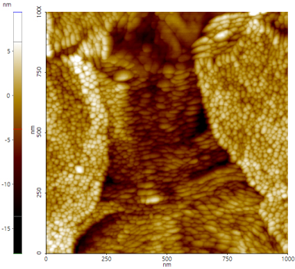
There are lots of techniques for characterizing the mechanical properties of sample, atomic force microscopy (AFM) has been widely used to investigate sample’s properties because it is able to measure Young’s modulus directly and quantitative measurement using force spectroscopy with contact mechanics models. From interactions between the AFM tip and the sample surface, the system collects that information and displays the output using force and distance units. In this presentation, we reviewed Park Systems’s mechanical properties measurement using AFM, with a particular emphasis on the “PinPoint nanomechanical mode”. This mode gathers topographical data at high resolution while simultaneously obtaining force-distance (FD) data at each pixel of the scan area. This allows sample surface morphology measurements while simultaneously obtaining quantitative nanomechanical properties such as modulus, adhesion, deformation, stiffness and energy dissipation.

Presented By :
Dr. Jake Kim, Park Systems Korea
Dr. Kim received Ph.D. degree in Materials Science and Engineering from Nanyang Technological University, Singapore. He joined Tokyo Institute of Technology International Research Opportunities Program (TiROP) in 2014 and was engaged in nano-scale chemical composition analysis using scanning probe microscopy (SPM). From December 2017, he started to work in Park Systems as the manager of application technology center. He is specialized in the enhancement of nano-machanical measurement performance for Atomic Force Microscopy (AFM), building up a accurate and reliable environment for electrochemical measurement using Scanning Probe Microscopy (SPM; SECM,SECCM) and Scanning Ion Conductance Microscopy (SICM) applications development for biology.
二次元半導体の成長と機能開拓
What is a good AFM in viewpoint of principle and applications?
LIVE WEBINAR!
2021년 6월 29일 화 오후 4시 (16:00 ~ 17:00)
*언어: 한국어 | This webinar will be presented in Korean.
SPM(Scanning Probe Microscope)은 나노 세계를 열어주는 최상의 장비이자, 가장 근본적인 기술입니다. 1세대 광학현미경과 2세대 전자현미경을 잇는 제3세대 현미경으로 알려진 SPM은 STM(Scanning Tunneling Microscope)의 발명에서 시작되었습니다.
STM은 프로브 팁과 진공 상태의 시료 사이의 터널링 전류를 사용하여 표면 토포그래피를 측정하므로 전도체 측정에만 국한되나, AFM이 개발되면서 다양한 범위의 측정이 가능하게 되었습니다.
대기 중의 부도체는 물론, 시료 표면의 물리적, 화학적, 기계적, 전기적, 자기적 특성 그리고 액상에서 살아있는 세포를 측정하는 것도 가능하게 되었습니다.
AFM은 나노기술 시대를 열어가는 중요한 도구이며, 나노과학기술연구 뿐 아니라, 첨단기술 제품개발 및 품질관리, 반도체 생산공정 등 다양한 분야에서 널리 활용되고 있습니다.
이번 웨비나에서는 AFM의 기본 원리 및 활용 방법에 대해 소개할 예정입니다.
AFM에 대해 더 자세히 알고 싶으신 분들은 지금 바로 등록해주세요!
Presented By :
김성오 박사 (Jake Kim, Ph.D.) | Application Scientist
Park Systems, Application Technology Center
김성오 박사는 싱가포르 난양 공과 대학에서 재료 공학 박사 학위를 받고, 2014년 TiROP(Tokyo Institute of Technology International Research Opportunities Program)에 합류하여 SPM(Scanning Probe Microscopy)을 사용한 나노 화학 성분 분석 연구에 참여했습니다. 2017년 12월부터 파크시스템스 본사 Application Technology Center에 Application Scientist 로 입사하여 AFM 측정, 테스트, technical article 작성 및 외부 강연 등 다양한 활동을 하고 있습니다.
原子間力顕微鏡による高分子ナノ力学物性の計測
Imaging modes of AFM from the application point of view
Tuesday, 15 Jun , 2021
- 10:30 AM
(ARAB)
Riyadh - 1:00 PM
(IST)
New Delhi - 3:30 PM
(SST)
Singapore - 5:30 PM
(AEDT)
Sydney
2021 SE Asia Webinar Series Schedule:
| Date | Topic |
|---|---|
| May 25 | Principles of AFM imaging modes |
| Jun 15 | Imaging modes of AFM from the application point of view |
| Jul 6 | Investigation of nanomechanical properties using AFM |
| Aug 10 | Crosstalk-free ferroelectric domain characterization via dual frequency resonance tracking PFM |
| Sep 7 | Scanning capacitance microscopy; advanced analysis for nanoscale semiconductor surface |
Understanding of surface structure and topography is essential for interpretation of material behavior at the nanoscale. To measure nano surfaces, different methods can be used such as confocal microscopy, scanning electron microscopy, transmission electron microscopy, and scanning probe microscopy (SPM). Atomic force microscopy (AFM) is a member in the SPM family that can measure various properties of samples in conjunction with their surface morphology. AFM allows quantitative measurement of surface features as small as angstrom level, which is relatively difficult to observe in conventional optical-based or electron beam-based techniques. To collect an AFM image, a sharp tip is typically used to sense the sample surface, and information on surface characteristics is accumulated by monitoring the tip-sample atomic interactions during scanning. Depending on specific applications, the AFM tip will come into direct contact (contact mode), intermittently contact (tapping mode), or scan over the sample surface at a given distance (non-contact mode). Contact, tapping, and non-contact are fundamental imaging modes of AFM. On the basics of these modes, various advanced techniques have been developed to measure different properties of samples such as electrical properties (C-AFM, KPFM, PFM modes, etc.), mechanical properties (nanoindentation, FD spectroscopy, and PinPoint modes), magnetic (MFM mode), and thermal (SThM mode) properties.
Within the scope of this webinar, practical applications of the imaging modes of AFM will be introduced. In addition, for better understanding on how AFM can measure your samples, a live session on imaging modes operations is also provided. It is expected that this webinar can be a useful material for gaining knowledge of AFM as well as its capabilities.
Presented By :
Rocky Nguyen, Park Systems Korea
Dr. Rocky Nguyen received his Ph.D. degree in Mechanical and Automotive Engineering from the University of Ulsan in South Korea and his Bachelor’s degree in Materials Engineering from Back Khoa University in Vietnam. He is currently focused on the development and performance optimization of atomic force microscopy and related techniques at Park Systems Korea.