シングルパスKPFMの原理詳細とハンズオンセッション
Park SmartScan™ - A point and click revolution in AFM imaging technology
Wednesday, 01 September, 2021
-
11:30 am
(ARAB)
Riyadh -
2:00 pm
(IST)
New Delhi -
4:30 pm
(SST)
Singapore -
6:30 PM
(AEDT)
Sydney
Atomic force microscopy (AFM) has become a more and more popular tool for nano-scale measurement across various field of studies. Using the AFM, sample’s properties can be measured and assessed to meet the requirements for each specific application. Despite the power and versatility, resistance that hinders the adoption of AFM remains. Conventional AFM operating softwares are relatively difficult to set-up and operate, especially for new user. To properly control the AFM, specialized trainings which require time and resources are required.
To reduce such efforts, Park Systems has built an innovative AFM operating software named SmartScanTM. The philosophy of SmartScan is to make AFM using experience as simple as point and click actions to control a computer. SmartScan has an Auto mode which implements automation in most of the steps required to get AFM image. User only need to set-up the tip and sample, point to a target area, and click a button to automatically collect the data. An expert-level high quality image can be obtained in only a fraction of time spent with the instrument. To achieve this, SmartScan employs the proprietary True Non-ContactTM imaging mode along with AdaptiveScanTM technique to automate and optimize the imaging procedure.
For cases that require repeated or multi-area measurement, Park StepScanTM function provides an easy set-up for automated measurements. User can add the area of interest by a simple mouse click while keeping full control of scan parameters such as scan mode, set point, scan size, speed, or resolution at each single area. This helps reducing the time spent with the instrument and leaving you more time for research.
In this webinar, we would like to introduce you the Park SmartScan AFM operating software. In particular, we will be presented the user interface and automation functions of the software. Also, a demonstration session on how to use the software to automatically measure the sample will be provided as a practical example.
Presented By :
Rocky Nguyen, Park Systems Korea
Dr. Rocky Nguyen received his Ph.D. degree in Mechanical and Automotive Engineering from the University of Ulsan in South Korea and his Bachelor’s degree in Materials Engineering from Back Khoa University in Vietnam. He is currently focused on the development and performance optimization of atomic force microscopy and related techniques at Park Systems Korea.
Scanning capacitance microscopy; advanced analysis for nanoscale semiconductor surface

Tuesday, 07 Sep, 2021
- 10:30 AM
(ARAB)
Riyadh - 1:00 PM
(IST)
New Delhi - 3:30 PM
(SST)
Singapore - 5:30 PM
(AEDT)
Sydney
2021 SE Asia Webinar Series Schedule:
| Date | Topic |
|---|---|
| May 25 | Principles of AFM imaging modes |
| Jun 15 | Imaging modes of AFM from the application point of view |
| Jul 6 | Investigation of nanomechanical properties using AFM |
| Aug 10 | Crosstalk-free ferroelectric domain characterization via dual frequency resonance tracking PFM |
| Sep 7 | Scanning capacitance microscopy; advanced analysis for nanoscale semiconductor surface |
Defining a dopant concentration been the key factor to understand a semiconductor device performance. In an effort of minimize scale of electric devices, memory devices or display panel has just a few nano size with atoms layered in 2D structure or 3D structure. To investigate these small structures, resolution is important as well as accuracy of measurement system.
Scanning capacitance microscopy (SCM) is the most adequate technique to measure the capacitance distribution on material surface which has the resolution of nanometer scale. Park systems’ enhanced scanning technique helps to acquire accurate capacitance signal without artifacts from tip-sample charging effect or stray capacitance noise.
In this talk, we demonstrate a full SCM analysis on a sample with various doping concentration range. In addition, advanced scanning method like ‘Quickstep’ and ‘Pinpoint’ will be adapted to the measurement to maximize accuracy and throughput of the data.

Presented By :
Zoe Kim, Park Systems Korea
Zoe Kim is an application engineer at Park Systems Korea, her role includes but is not limited to surface inspection and mechanical lithography on display panel, semi-conductor devices, and battery samples with electrical, mechanical, and thermal analysis. She is also assigned in writing technical articles for publications. She received her Bachelor's Degree in Physics from Incheon National University and her Master's degree from Sungkunkwan University, South Korea.
圧電応答測定(PFM:Piezoelectric Force Microscopy)
原子力显微镜在钙钛矿太阳能电池界面修饰中的应用
2021年7月8日*星期四
北京时间东八区上午10:00-11:00
*Note: This webinar will be presented in Mandarin /中文
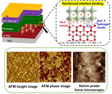
左上图为平面正式钙钛矿太阳能电池的结构图,由透明导电玻璃(ITO)
/电子传输层(ETL)/活性层(perovskite)/空穴传输层(HTL)
/背电极(Au)构成;右上图为氟功能化氧化钛上的氟和钙钛矿相互作用的示意图,二者形成Pb-F键和N-H⸱⸱⸱F键,加强了界面键合。
下图是由Park XE-7拍摄的三幅不同类型的图,第一幅是氧化钛的形貌图,第二幅是钙钛矿活性层的相图,第三幅是钙钛矿的电势图(KPFM)
原子力显微镜(AFM)是最强大的扫描探针显微镜(SPM)技术之一,其不仅可以探测薄膜的形貌,而且可以表征薄膜的相组成和表面电势,广泛用于能源领域。同时,钙钛矿太阳能电池因其制备简单、高效廉价,近些年引起了人们的广泛兴趣,其认证效率现已达到25.5%。然而此效率与S-Q理论预测的极限效率仍有一定的差距,这主要是由界面的缺陷态造成的非辐射复合引起的,故精心调控钙钛矿太阳能电池的界面非常必要。因此,AFM被广泛应用于钙钛矿太阳能电池中,来揭示界面修饰引起的形貌、能级及相互作用的改变,从而找到界面修饰对器件性能影响的内在因素。而本次网络研讨会将从两个方面进行: 1)AFM的哪些功能可以用来表征钙钛矿太阳能电池? 2)如何利用AFM揭示界面修饰对钙钛矿太阳能电池性能提升的内在机理? 3)原子力显微镜在以氟功能化TiO2为电子传输层的有机-无机杂化钙钛矿太阳能电池中的具体应用。

主讲人:
胡万培博士
胡万培,中国科学技术大学材料系博士,师从杨上峰教授。主要研究方向是有机无机杂化钙钛矿太阳能电池的界面改性和新型无铅钙钛矿太阳能电池。以第一作者在Advanced Materials, Nano Energy, Trends in Chemistry, Advanced Science上发表研究论文4篇。